I'm always have an eye on what's edge computing's going on because I'm a fan in IoT. Honestly, I start doing my CS major with IoT projects though it was very dump.(listed is not my first dump project hhhhh)
I prepared to do sth in SHIFT, also congratulations to Prof. Yang's recent publication:
Multi-tier computing networks for intelligent IoT. But the S3L first respond to me, So I'm a security guy right now.
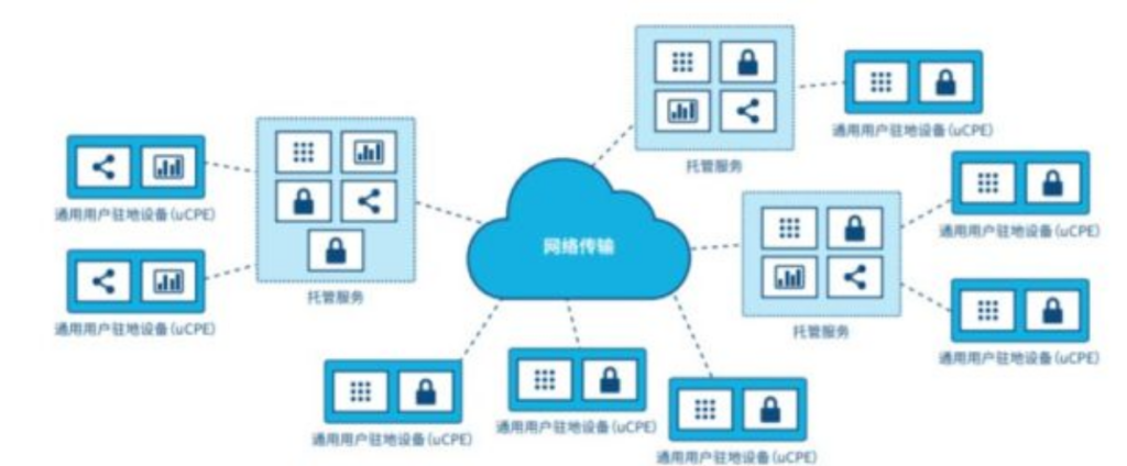
I've been upon thinking the idea for a while, the idea of the problem is very similar to the state of art key problems.
1. Computing power: data processing equipment is no longer a rack server, how to ensure that the performance meets the requirements
2. Power consumption: power consumption cannot be as large as the level that ordinary civil power is difficult to accept, and power consumption also means that the heat is large
3. Stability: deployment outside causes the difficulty of field maintenance to increase dramatically The improvement of stability also means the reduction of maintenance cost, which also includes the harsh environment on the user side, such as high temperature, humidity, corrosive gas, etc.
4. Cost: only the cost can cover the demand, can we deploy and meet the customer demand as much as possible, if the cost is not comparable to the network + data center, it is meaningless
Moore's law has met with a bottleneck. It is more and more difficult to make the best of both general and specific optimizations. At this time, the hardware coprocessor which integrates common AI algorithms directly in edge computing becomes the key to obtain high performance and low power consumption. A key threshold for power consumption is 6W TDP. Generally, in the design, the power consumption of the chip is less than 6W, and the fan can not be used with the heat sink. The absence of fans not only means the reduction of noise, but also means that the stability and maintainability are not affected by fan damage. In the front-end chip of edge computing class, horizon based on its self-developed computer architecture BPU has found a new balance point in various requirements. The equivalent calculation power of 4 tops provided by it has reached the calculation power of the top GPU two years ago, while the typical power consumption is only 2W, which means that not only fans are not needed, but also the whole machine can be installed in the metal case to avoid dust and corrosion caused by redundant holes.
When it comes to computing power, there is a big misunderstanding in the current industry, which often takes the peak computing power as the main index to measure the AI chip. But what we really need is the effective computing power and the algorithm performance of its output. This needs to be measured from four dimensions: the peak computing power per watt and the peak computing power per dollar (determined by chip architecture, front and rear end design and chip technology), the effective utilization rate of peak computing power (determined by algorithm and chip architecture), and the ratio of effective computing power to AI performance (mainly in terms of speed and precision, determined by algorithm). RESNET was widely used in the industry before, but today we use a smaller model with more sophisticated design like mobilenet, which can achieve the same accuracy and speed with 1 / 10 of the calculation force. However, these ingenious design algorithms bring huge challenges to the computing architecture, which often make the effective utilization rate of the traditional design of the computing architecture greatly reduced, and from the perspective of the final AI performance, even more than worth the loss. The biggest feature of horizon is to predict the development trend of key algorithms in important application scenarios, and to integrate its computing features into the design of computing architecture prospectively, so that the AI processor can still adapt to the latest mainstream algorithm after one or two years of research and development. Therefore, compared with other typical AI processors, horizon's AI processor, along with the evolution trend of the algorithm, has always been able to maintain a fairly high effective utilization rate, so as to truly benefit from the advantages brought by algorithm innovation. Horizon also optimizes the compiler's instruction sequence. After optimization, the peak effective rights are increased by 85%. This makes the processing speed of the chip increased by 2.5 times, or the power consumption reduced to 40% when processing the same number of tasks. Another feature of horizon BPU is that it can be better integrated with sensors in the field. Video often requires huge bandwidth. 1080p @ 30fps video has a bandwidth of 1.5gbit/s from camera to chip. And horizon BPU can complete the video input, field target detection, tracking and recognition at the same time, so that all necessary work can be completed on site. Both the journey series applied to intelligent driving and the sunrise series applied to the intelligent Internet of things can easily cope with the huge bandwidth and processing capacity of the scene. More importantly, the common AI calculation can be completed in 30ms. It makes the applications that are extremely sensitive to time delay become reality gradually, such as automatic driving, recognition of lane lines, pedestrians, vehicles, obstacles and so on. If the time delay is too large or unpredictable, it will cause accidents.
However, by using sunrise BPU, AI calculation can be completed within predictable time delay, which can make the development of automatic driving more convenient. The application of edge computing has been limited by the performance of computing, the strict limitation of sensors and power consumption since it was put forward, and the development of edge computing is slow. And horizon BPU series chips, seeking a new balance in function and performance, can also effectively help edge computing applications to be more easily deployed to the site, so that all kinds of Internet of things applications can more effectively serve everyone.
